In Industrial manufacturing, and particularly in the semiconductor industry, High-Performance Computing (HPC) is enabling advancements in miniaturization, speed, and energy efficiency. As this sector continues to evolve, the computational demands have not only increased but have also become more specialized, encompassing intricate simulations for material science, complex calculations for electronic design automation (EDA), and data-intensive tasks like nanomaterial imaging and defect analysis.
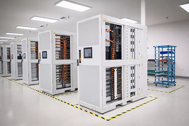
In this context, HPC solutions serve as the backbone of computational capabilities, enabling semiconductor firms to fuel advancements in chip design and rapid output. The role of HPC is critical not just in accelerating computational tasks but also in ensuring the precision and accuracy that are non-negotiable in semiconductor manufacturing and design. From optimizing silicon wafer yields to enabling real-time analytics for quality control, HPC solutions are integral to the industry’s drive for innovation and operational excellence.
Computational Demands in Semiconductor Manufacturing
In the semiconductor manufacturing sector, computational demands are both diverse and highly specialized, requiring High-Performance Computing (HPC) solutions that can handle a range of complex tasks. One of the most critical areas is material science, where intricate simulations are essential for understanding the properties and behaviors of semiconductor materials at the molecular and quantum levels. These simulations often involve molecular dynamics for assessing material properties and quantum mechanical simulations for evaluating electronic properties. The computational load for these tasks is immense, requiring robust CPUs, GPUs, and sometimes even specialized accelerators to perform efficiently.
Another significant computational area is EDA, which involves complex calculations for circuit simulation, timing analysis, and logic verification. These tasks are crucial for ensuring that semiconductor components meet the desired specifications and quality standards. In addition to EDA, data-intensive tasks like nanomaterial imaging and defect analysis are becoming increasingly important. These tasks require not only high computational power but also substantial data storage and high-speed data transfer capabilities. Software tools for these data-intensive tasks often include advanced data analytics platforms and machine learning algorithms specifically designed for defect detection and quality control.
Nanomaterial Imaging
Now, let’s use a real-world example to figure out the total computing power needed to carry out a nanomaterial imaging job over the full 1keV to 30keV energy range. Please note these numbers are from September 2023, these are expected to change greatly as available hardware evolves.
Estimated Computational Requirements for Nanomaterial Imaging:
- Resolution: 0.6 nm
- Image Size: 6144 x 4096 pixels
- Operations Per Pixel: 1000 operations (for defect detection analyses)
- Total Operations per Image: 6144×4096×1000
To achieve real-time inspection with a dwell time of 25 ms per pixel, the total operations translate to: 983TFLOPS (TeraFLOPs).
Harnessing a Standard HPC Rack:
A typical 42U rack accommodating 21 2U 4Nodes servers, each node equipped with dual Intel® Xeon® Platinum 8380 Processors, yields around 193TFLOPS. For this scenario, to meet the demanding 983TFLOPS workload, approximately five racks would be required.
Scalability
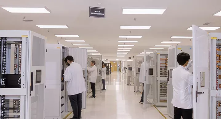
Scalability is an essential consideration in the deployment of HPC solutions within the semiconductor industry. Given the high-throughput nature of semiconductor manufacturing processes, the computational infrastructure must be designed to scale efficiently. Advanced equipment in these facilities, often responsible for tasks like wafer processing and defect analysis, generate immense computational loads. The ability to scale resources up or down in response to these demands is not just an advantage; it’s a requirement for maintaining operational efficiency.
Let’s use the S5000-10 Floor-standing sorter, capable of processing up to 350 wafers per hour (WPH) when reading laser marks, as an example. In a typical semiconductor facility, a single advanced equipment such as S5000-10 Floor-standing sorter from C&D Semiconductor Service can process up to 350 wafers per hour (WPH) when reading laser marks
Let’s estimate the estimated workload with such S5000-10 with a hypothetical scenario
- Estimated Workload for S5000-10:
- Dies per Wafer: 300
- Images per Die: 2
- Images per Wafer: 600
- Wafers per Hour: 350
- Images per Hour: 600×350=210,000
- Total TFLOPS Required per Hour: 983×210,000=206,430,000TFLOPS or 206,430PetaFLOPS
- To keep pace with the S5000-10, about 210,000 racks of the aforementioned configuration would be necessary, underscoring the imperative of scalability in HPC infrastructure.
Customization
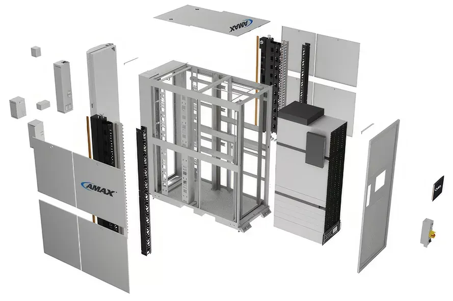
Tailored HPC solutions are vital for meeting the unique and ever-changing demands of semiconductor companies. As the industry advances, requiring increasingly intricate computations and simulations, an adaptable HPC infrastructure becomes indispensable. This adaptability encompasses hardware setups, software configurations, and network arrangements, all designed to proficiently manage the varied workloads and data tasks integral to semiconductor research and production.
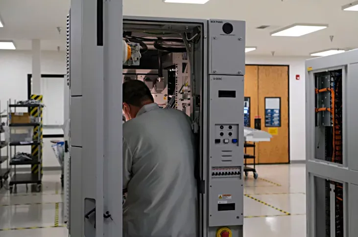
In the semiconductor industry, a sector that significantly influences technological progress across the IT landscape, customization of standard IT equipment is often necessary. For example, regulations stipulate that an Emergency Off (EMO) button must be within 3 meters of each operational and maintenance area. Moreover, as semiconductor facilities elevate their ESG standards, new criteria like complete heat removal from deployed HPC solutions on the production floor are emerging. Additionally, environmental risks such as seismic activity must be considered, requiring HPC solutions to comply with the most stringent guidelines, like the USGS Seismic Zone 4 requirements.

Longevity in HPC
Longevity in High-Performance Computing (HPC) deployment is a critical factor that directly impacts the Total Cost of Ownership (TCO) for semiconductor companies. A long-lived HPC infrastructure means fewer disruptions in operations, which translates to increased productivity and reduced downtime costs. Additionally, a durable setup minimizes the frequency of hardware upgrades and replacements, allowing companies to amortize their initial investment over an extended period. This financial stability is crucial for maintaining a competitive edge in a rapidly evolving industry.
Moreover, an HPC infrastructure designed with longevity in mind is inherently adaptable. It can accommodate emerging technologies and workloads without requiring a complete overhaul. This adaptability ensures that semiconductor companies can stay ahead of technological advancements, thereby maintaining their competitive and innovative edge over time. AMAX Engineering, with its global reach, ensures that its HPC solutions are not only long-lasting but also compliant with a myriad of local regulations, including FCC standards in the United States, KCC in South Korea, and BSMI in Taiwan.
Global Infrastructure Deployment
The semiconductor industry is inherently global, with operations often spread across multiple continents. This geographical diversity requires a standardized global deployment framework for HPC infrastructure. Such a framework ensures consistency in performance, operational efficiencies, and compliance with both regional and international regulations. Standardization is vital for maintaining quality control and for the seamless integration of various operational units spread across different parts of the world.
A globally deployed HPC infrastructure also enables seamless collaboration among teams, irrespective of their geographical locations. This is crucial for data sharing, resource optimization, and overall enterprise efficiency. The ability to collaborate in real-time across different time zones and regulatory environments can significantly accelerate R&D cycles and time-to-market for new products. AMAX Engineering’s global deployment capabilities ensure that its HPC solutions meet these complex requirements, offering a harmonized approach to HPC infrastructure that is both efficient and compliant with international standards.

Compliance, Regulations, and Safety
in the semiconductor industry, the regulatory environment for High-Performance Computing (HPC) solutions is both stringent and complex, demanding a multi-faceted approach to compliance and safety. Key industry standards such as SEMI S2, S8, and F47 set the guidelines for environmental, health, and safety aspects, including the safe operation of semiconductor manufacturing equipment. These standards often dictate the design and operational parameters for HPC solutions deployed in semiconductor fabrication plants. Additionally, compliance with the National Fire Protection Association’s NFPA 79 standard is crucial, as it outlines the safety requirements for industrial machinery, including electrical and control aspects. Failure to adhere to these regulations can result in not only legal repercussions but also operational inefficiencies and increased risk factors.
For example, SEMI S2 (Environmental, Health, and Safety Guideline for Semiconductor Manufacturing Equipment) has several key requirements for any HPC solutions to meet, such as:
- Emergency Shutdown: The standard mandates that an Emergency Off (EMO) button should be accessible within 3 meters (10 feet) of each use and maintenance location.
Noise Levels: The standard specifies that noise levels should not exceed 85 dBA when measured at 1 meter from the equipment and at a height of 1.5 meters from the floor. - Electrical Safety: Electrical components must be designed and installed to prevent electrical shocks, fires, and other hazards. This often involves the use of circuit breakers, grounding, and other safety mechanisms.
- Ventilation and Air Quality: Adequate ventilation must be provided to ensure that any fumes or particulates generated during operation are effectively removed, maintaining air quality within safe levels\
Case Study
Overcoming challenges in the Semiconductor Industry
Client
A leading semiconductor manufacturer with a global footprint, specializing in a diverse range of semiconductor products.
Challenge
The client operated in an environment with extreme condition requirements, including seismic considerations, regulatory compliance, environmental sustainability, heat management, and safety protocols. These factors created a complex web of challenges that traditional computing solutions could not adequately address.
Solution
AMAX engineered a High-Performance Computing Cluster specifically tailored to meet the client’s multifaceted challenges. The solution incorporated:
- Seismic-Resistant Design: Custom-built racks and enclosures designed to withstand seismic activities, ensuring operational continuity in geologically sensitive areas.
- Regulatory Compliance: Systems configured to meet all local and international regulatory standards, including data protection and environmental regulations.
- Advanced Cooling Systems: Implementation of liquid cooling technologies, including D2C and RDHx, to manage heat effectively, even under peak load conditions.
- Safety Measures: Integration of advanced fire suppression systems, electrical fail-safes, and leak protection, to ensure the highest levels of safety.
- Eco-Friendly Components: Utilization of energy-efficient components to minimize environmental impact and comply with sustainability goals.
Outcome
The custom-engineered High-Performance Computing Cluster successfully met all the client’s stringent requirements:
- Achieved full compliance with seismic, regulatory, environmental, and safety standards.
- Reduced heat-related incidents by 90%, thanks to the advanced cooling systems.
- Realized a 35% reduction in energy consumption, aligning with the client’s sustainability goals.
- Enhanced overall system reliability, leading to a 20% increase in operational uptime.
AMAX’s custom-engineered HPC Cluster proved to be a game-changer for our client. Not only did the solution meet the stringent requirements of seismic resilience, regulatory compliance, and environmental sustainability, but it also delivered tangible results—reducing energy consumption, enhancing system reliability, and significantly improving operational uptime. This case study underscores the transformative impact of a well-designed, tailored HPC solution in overcoming the multifaceted challenges that semiconductor manufacturers face. With AMAX’s expertise, clients can confidently navigate the complexities of their industry, achieving both compliance and performance excellence.

